Introduction
A few months ago – as a prototyping experiment – we decided to develop two types of high-power switching boards: one for high-side switching and another one for low-side switching. Goal was to gain some experience on different switching techniques for charge controllers.
We contacted several hardware development / prototyping companies and, at the same time, we created projects on freelancer.com and elance.com. The low-side switching project was given to IACS while the high-side project was assigned to an Ukrainian guy on elance.com. Read this post for more detail on the low-side switching project.
Elance experience
So, we gave our ‘go’ to the high-side switching project and development started. For those who are not familiar with elance’s way of working: a project is supposed to have several milestones, and each milestone results in a payment (of course, both parties have to agree before money flows). It is also possible to change terms and milestones. This system works quite well because projects tend to change scope :-).
We defined four milestones:
- solid specification: since we are no hardware engineers, it is not easy for us to write clear hardware specs. Therefor, we prefer to do this together with the hardware engineer.
- PCB design
- 4 additional prototypes: this milestone was added later in the project. Initially, we only ordered 4 prototypes which is not enough in case of issues. This milestone brought the total amount of prototypes to 8.
- final deliverable
The last milestone ‘final deliverable’ is an interesting one. Its details say:
… After a short test period (7 days), the deliverable is accepted or rejected. Support from the freelancer in order to fix shortcomings and bugs is expected. …
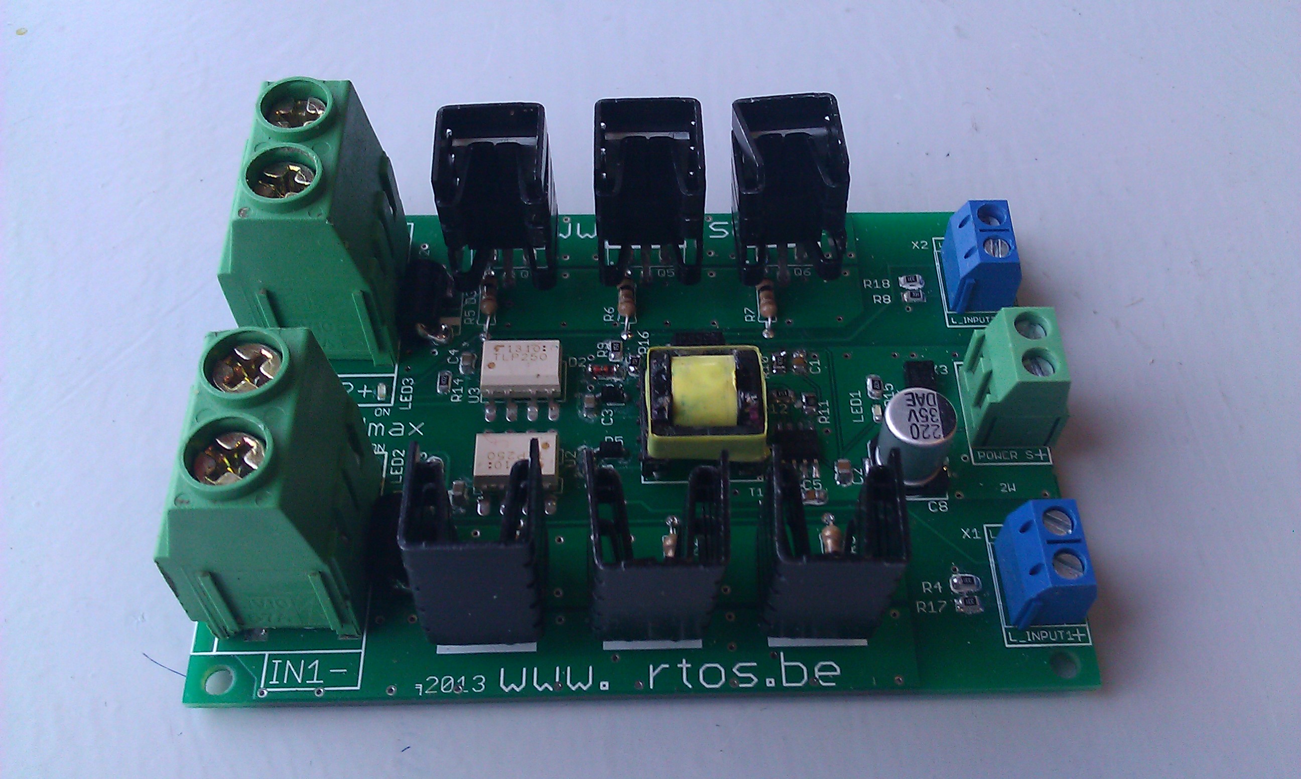
All well up to milestone 3. The design of one high-side switching channel was based on two or three N-channel mosfets which were driven in parallel. In order to get Vgs correct, the board implemented (and still has) a gate drive transformer via an isolated power supply (see yellow block on the picture; read here about Voltage Level Shifting).
When the boards arrived and we did our initial tests, results were quite bad, especially when applying PWM (one of our requirements). Even at low PWM frequencies:
- mosfets were burned,
- TVSs (iow Transient Voltage Suppressors; the black thing behind each connector) were destroyed.
Some basic investigation revealed that:
- the mosfets of one channel sometimes had more than 20 degrees difference in temperature (so are they really driven in parallel?)
- there was quite some voltage under/overshoot… see pictures.
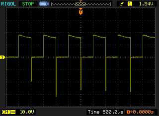
pwm: 1kHz, duty cycle: 50%, load: 80W

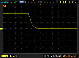
end of block wave, pwm: 1kHz, duty cycle: 50%, load: 80W
For your reference, this is how it looks on our low-side switching board (but we have to say it has more protection features):
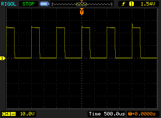
Our freelancer clearly didn’t test the board… 🙁 We told him our findings but till today we didn’t get any answer… And therefor we decided not to pay for milestone 4.
Board issues
So we asked our Belgian hardware engineer to have a look at the board. His findings were:
- Conceptually the design is good.
- Voltage rating of the FETs are not ok. A rule of thumb is to apply a 20% derating on mosfet’s breakdown voltage.
- The used optocoupler is at the end of its life: “not recommended for new designs”. A decouple capacitor is missing.
- Grounds of the two channel are not tied together at pcb level, although this is the case in the schematics. Probably not an issue though.
- A large amount of turn-on and turn-off ringing caused by a too small gate resistor and possibly not-so-good design.
Board improvements
At first, the number of FETs per channel was reduced to one. This simplifies the design and eases debugging.
Secondly, the underrated FETs were replaced, and other mosfet types were tested and compared e.g.
- Infineon IPB037N06N3 G
- IRF irfs3206pbf
- NXP PSMN5R0-80PS
Best results were obtained with NXP mosfets.
Finally, a lot of time was spent on mitigating turn-on and turn-off ringing. Next solutions have been tried out:
- Adding a capacitor parallel to drain and source. By adding a large capacitor a good effect was noticed on the turn-on ringing. The turn-off was impacted but at a lower level.
- Adding a snubber network (RC a C to tune to the parasitics of the LC network, the R is added to dampen the oscillation) tuned to the circuits parameters. This has had a low impact on decreasing the ringing.
- Changing the gate resistor to slow down to on/off switching. Together with a parallel drain-source capacitor this had a good effect on turn-on, less on turn-off ringing.
- Dividing the gate resistor into a turn-on part and a turn-off part. The MOSFET will switch on fast (turn-on is not a big problem in the circuit). When the MOSFET is switched off it will be slower. A big drawback for this solution is that it will decrease switching efficiency (the component is a long time active in its linear area) which results in more heat generation.
At the end of our test cycle, results improved dramatically! Battery charging with PWM went very well.
What’s next
A test board, schematics and our findings have been sent to IACS for further test. We might sell this board in the future as well.

The high side mosfet driver module can be used at %100 duty?
and How can ı buy it? just 3 or 4 pcs
Please use the contact form and request a quote for the amount of high side switching boards required. We will reply with a price for the boards and shipping (please provide your shipping address). Commercialization was delayed because of other priorities, but the prototype boards have been tested and approved by us. The test results are quite impressive although we will decrease the “official” maximum supported voltage, amperage and power ratings somewhat: but 2 channels at 50V, 50A and 2500W at any pwm rate (0 to 100% dc) at 100Hz (250 or 500Hz might be possible depending on your application) should not be any problem. The prototype board passed much harder tests. A more detailed article about the high side board follows, if we can find some time to write it 🙂
One more remark: our low-side switching board might be suitable for your application as well. Currently, there are still 5 pieces available.
Please follow this link (specs are available for download):
http://www.ebay.co.uk/itm/RTOS-BE-IACS-Energy2Switch-2-Channel-MOSFET-N-Channel-Switch-Board-1500W-50V-40A-/171296385473?